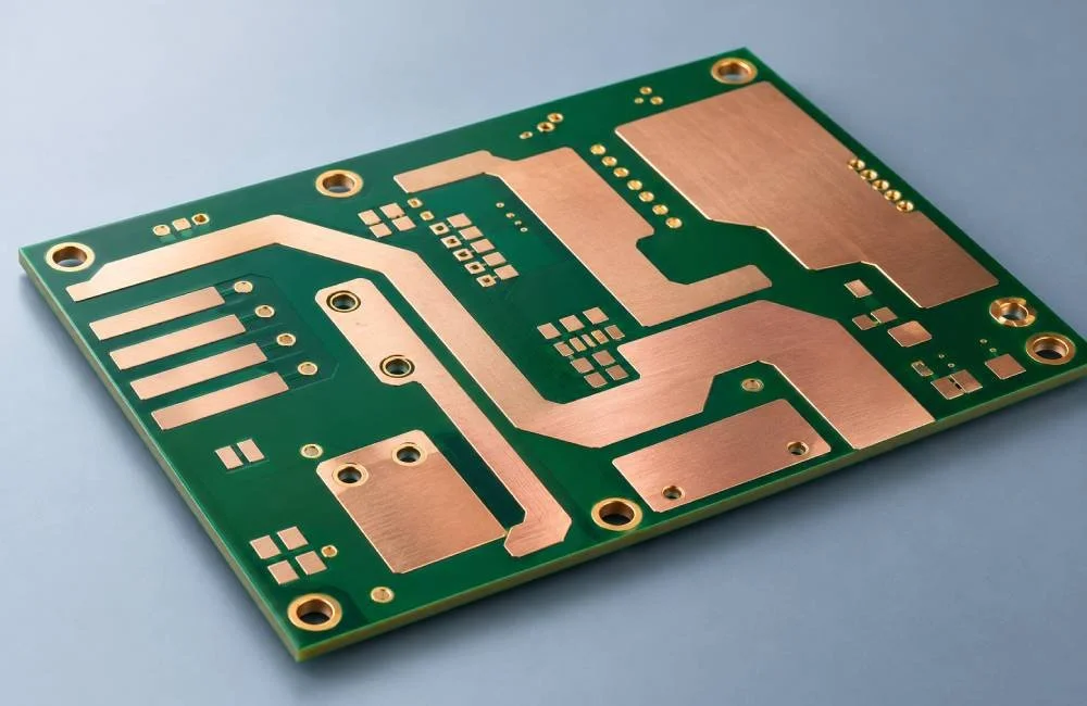
Manufacturing overview
Heavy-copper designs require copper thickness, circuit geometry and thermal requirements to be reviewed together. State the finished copper requirements separately for inner and outer layers.
Copper changes the geometry
The finest line and spacing values cannot automatically be combined with the highest copper weight. Submit the actual layout and copper specification for a construction-specific review.
Include the full manufacturing scope
Confirm layer construction, finished thickness, holes, finish and acceptance requirements. Identify any current-related or thermal requirements that constrain material or process choices.
Heavy copper changes more than the copper weight
Heavy-copper construction is considered for power distribution and thermal requirements. Greater copper thickness changes etching, plating, feature spacing and solder-mask requirements. A copper-weight value alone does not establish current-carrying capacity; the circuit geometry, temperature rise and operating conditions must also be assessed.
| Heavy-copper input | What to specify |
|---|---|
| Finished copper | Inner and outer layer requirements, identified separately. |
| Circuit geometry | Critical conductor widths, spaces and local density. |
| Stackup balance | Copper distribution and finished board thickness. |
| Acceptance | Hole requirements, inspection and any required records. |
What to include in your quotation request
Provide the fabrication package and drawing at one revision. Distinguish fixed requirements from items open to engineering proposals. Include quantity and the required ship or arrival date; the material, construction and verification scope must be reviewed before the delivery plan is confirmed.
- Fabrication artwork, drill data and mechanical outline.
- Stackup, material grades and finished copper requirements.
- Surface finish, critical tolerances and special features.
- Required inspection, test conditions and documentation.
- Quantity, project stage, destination and date requirement.
Questions, answered
Before your next build
What should I include in the quotation package?
Send fabrication and drill data, a drawing, stackup or construction details, quantity, material and finish requirements, and the required ship or arrival date.
Can copper weight alone determine the current rating?
No. Current capability also depends on conductor geometry, allowable temperature rise and the operating environment. Provide the electrical and thermal design constraints.
Are the same fine features available at every copper thickness?
Do not assume so. Increased copper changes the manufacturing requirements for lines, spaces and other features. Review the geometry against the specified copper construction.