What controlled impedance means
A controlled impedance specification connects a transmission-line target to a defined PCB construction. Trace geometry, copper, dielectric thickness, material properties and reference planes must be considered together. High-speed digital and RF designs can require this control, but the circuit designer must determine the appropriate targets.
Turn a target value into a manufacturable requirement
A note such as “controlled impedance” is incomplete. Identify the signal structure, target value, tolerance and applicable layers. For differential pairs, include the spacing requirement and reference construction as well as the trace width.
| Input | Example of the required detail |
|---|---|
| Signal structure | Single-ended or differential; surface or embedded routing. |
| Layer relationship | Signal layer and reference plane or planes. |
| Target | Required impedance and permitted tolerance for each structure. |
| Material construction | Grade, dielectric thickness and finished copper. |
| Design authority | Which geometry changes may be proposed and who must approve them. |
Stackup review before release
Review the proposed stackup before final fabrication approval. If a manufacturer proposes a trace adjustment to meet a target, confirm that the change is compatible with the design. Impedance engineering does not replace channel simulation or system-level signal-integrity validation.
Coupons, TDR and reporting
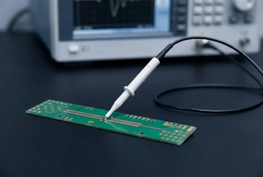
Impedance coupons, time-domain reflectometry and measurement reports can be included in a project-specific verification plan. Specify the required verification when requesting a quotation, including which structures must be represented and what records are needed. A coupon measurement should be interpreted within its agreed test construction and acceptance criteria.
Keep impedance control separate from continuity testing
An electrical connectivity test checks intended connections and isolation. It does not by itself establish characteristic impedance. If a project needs both connectivity and impedance verification, state both requirements in the fabrication package.
Questions, answered
Before your next build
Does an electrical test verify impedance?
Continuity and isolation testing does not by itself establish characteristic impedance. Specify the impedance structures and verification separately.